Product introduction
BGA full name Ball Grid Array literally translates to ball grid array package;
Product characteristics
The use of flip chips can increase the amount of I/O, in a smaller space for more signal, power and power supply interconnection;
High package reliability, low defect rate of solder joint (< 1ppm/ solder joint), solid solder joint;
Shorter interconnection path, reduced inductive reactance/impedance/capacitive reactance, reduced signal delay, and better high-frequency signal transmission performance;
Use environmentally friendly materials, in line with RoHS standards;
Apply
Storage, CPU, GPU, graphics acceleration chip, server, etc.;
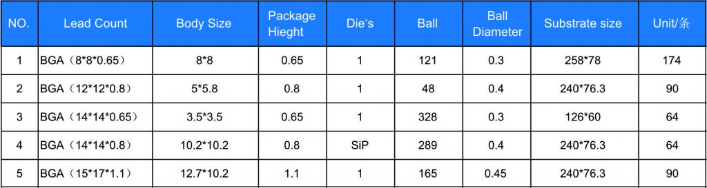
Process characteristics
The outer leads of the BGA package products are welding balls or welding bumps, which are distributed in an array on the bottom plane of the package substrate, on which a large-scale integrated circuit (LSI) chip is assembled, which is a surface assembly package type of LSI chip. There are two common interconnection methods, lead bonding (WBBGA) and reverse welding (FCBGA).
The high yield of BGA products can reduce the failure rate of narrow-spaced QFP solder joints by two orders of magnitude, significantly increase the number of leading terminals and body size ratio, and high interconnection density;
BGA pin short, good electrical performance, firm, not easy to deformation; The welding ball effectively improves the coplanarity and helps to improve the heat dissipation.
BGA can support thousands of I/ OS, and the most typical application is Intel CPU packaging.